Simple FPGA Pokémon Battle Game
Published:
Introduction
In this project, I built a VGA controller to display a simplified version of a Pokémon battle sequence using SystemVerilog on an FPGA. The user will be able to select one of four Pokémon to match up against the opponent (in this case, an NPC). This project was completed as part of my coursework for Virginia Tech’s ECE 4514 Digital Design II class, and implemented on an Altera DE1-SoC board.
Game Play and Controls
Using a Linear Feedback Shift Register and the Fisher Yates Algorithm, the sequence of the opponents Pokémon is shuffled each reset. The LFSR uses a counter as a seed and generates a new index that is then used to shuffle the numbers preplaced in the array. Each of the opponents 4 Pokémon have a corresponding number, 1, 2, 3, or 4. These numbers are shuffled at system reset and change based on whether the player has won a matchup. The User will use one of the FPGA key buttons to advance the states. Once the Pokeball appears on the user side, the User will flip one of SW [3:0] to select a Pokémon, advancing the state will display that Pokémon, and then the system will check if the user won the battle. A losing matchup would display a small red square to the left, while a winning match displays a green square. As there are 4 Pokémon per side, if either of the sides win 4 times, the game will end. The screen will turn green for a player win or red for a player loss.
VGA Controller
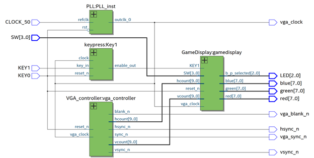
The VGA controller is responsible for generating the necessary signals to drive a VGA display. It generates the horizontal and vertical synchronization signals, as well as the pixel clock. The controller also manages the timing of the display, ensuring that the pixels are drawn in the correct order and at the correct time. As the screen we will be using is a 640x480p, 60Hz display, we will need to create a Phase Locked Loop (PLL) to generate a VGA clock signal. To find the target frequency of the PLL, we multiply 800 x 525 x 60 to reach a frequency of 25.2 MHz, to count each pixel within the visible and nonvisible areas 60 times a second. We use 800 and 525 as they are the total number of pixels in a row and column, respectively, including the visible and nonvisible areas. The visible area is 640x480, while the nonvisible area is made up of the front porch, sync pulse, and back porch. The front porch is a small area before the sync pulse that allows the display to prepare for the next line or frame. The sync pulse is a signal that tells the display when to start drawing a new line or frame. The back porch is a small area after the sync pulse that allows the display to finish drawing the current line or frame before starting the next one. Below is the system architecture of the VGA controller, connected to the GameDisplay module. 
Game Logic and Design
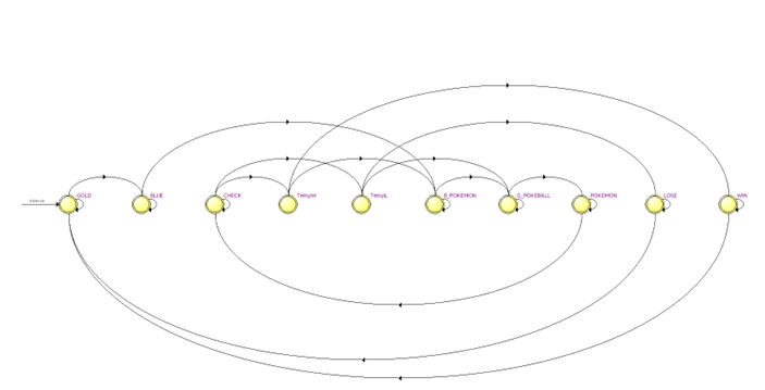
Each sprite is held in its own ROM, where the address is defined by the hcount and vcount values used by the VGA controller. To create the ROMs, a python script was created to extract the color value for each pixel, and the output the data in the form of a case structure that acts as a ROM. The sprites are “activated” according to the order defined by the controller FSM, once activated the sprites are displayed in a set area on the screen. In total there are 11 total sprites, ranging from 48x48 pixels to 56x56 pixels. The sprites include the 4 player Pokémon, 4 opponent Pokémon, a Pokéball, and win/loss indicators. The game controller FSM is responsible for managing the state of the game, including the current Pokémon selected by the user, the opponent’s Pokémon, and the win/loss status. The User iterates the states using KEY [1] on the DE1 SoC, selects their Pokémon during the “G_POKEBALL” state, and then checks if the matchup ended in a victory. There are temporary states for the win and loss counters to avoid incorrect state transitions. Each of the states has control over Sprite enable signals, which determines when sprites are displayed on screen. Each of the sprites has a pre-determined location where they appear. Below is the state diagram for the game controller FSM. 
Gameplay
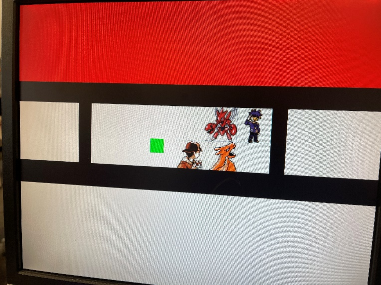
Once the RTL is synthesized and loaded onto the FPGA, the user can interact with the game using the buttons and switches on the DE1-SoC board. First, the user must use KEY [0] to reset the game, which will shuffle the opponent’s Pokémon and display the starting screen. Using KEY[1] will advance the game and display your opponent’s Pokémon. When the Pokéball appears on the user’s side, the user can select their Pokémon using SW [1:0]. The game will then check if the user won or lost the matchup and display the corresponding indicator. The example below shows the user winning the matchup. 
FPGA Resource Utilization
The project was implemented on an Altera DE1-SoC board, which features an Intel Cyclone V FPGA. The resource utilization for the project is as follows:
| Resource Type | Used | Available | Utilization (%) |
|---|---|---|---|
| Logic Elements | 15,472 | 32,070 | 48% |
| Registers | 135 | N/A | —– |
| PLLs | 1 | 6 | 16.67% |
| Pins | 39 | 457 | 8.54% |
Further improvements could be made to the game by adding more Pokémon, implementing animations, and developing a Frame Buffer to properly use FPGA memory resources.
