Izhekich Neuron based Spiking Neural Network Template
Published:
Introduction
With the rise in power consumption in high-performance computing, the demand for energy-efficient systems is increasing. Neuromorphic computing with FPGAs aims to bridge the gap between current GPU-based machine learning and future neuromorphic hardware. Spiking Neural Networks (SNNs) are the third generation of neural networks, more closely mimicking the human brain by using discrete spikes to transmit information, unlike traditional artificial neurons that use continuous values. This project implements a spiking neural network for character recognition using Izhekich neurons on an FPGA. The Izhekich neuron model is a simplified version of the Hodgkin-Huxley model, describing the electrical activity of neurons in the brain. It is computationally efficient and suitable for FPGA implementation with limited resources. This was the final project for Virginia Tech’s ECE 5404 Advanced Analog IC Design course.
Previous Work
This project aimed to develop the SNN described in [1] and use the FPGA implementation of the Izhekich neuron model from [2]. This network consists of an input layer and a fully connected output layer to classify a set of 48 alphanumeric characters. The number of input neurons is equal to the number of pixels in the input image (A 24x24 image has 576 pixels), and the number of output neurons is equal to the number of classes (48). The researchers in [1] developed a custom RTL design to compute the neurons’ membrane potential through a set of processing elements, rather than developing a custom neuron module and instantiating it multiple times. In [2], the researchers propose a FPGA optimized version of the Izhikevich neuron model, which use fixed-point arithmetic and optimizes certain operations by using shift operations instead of multiplication or division.
Izhekich Neuron Model
The Izhekich neuron model is described by the following equations: \(\frac{dV}{dt} = 0.04V^2 + 5V + 140 - u + I\)
\[\frac{du}{dt} = a(bV - u)\] \[\text{if } V \geq 30 \text{ mV, then } \begin{cases} V &\leftarrow c \\ u &\leftarrow u + d \end{cases}\]Where:
- ( v ): Membrane potential of the neuron
- ( u ): Membrane recovery variable
- ( I ): Input current
- ( a, b, c, d ): Parameters defining the neuron’s behavior
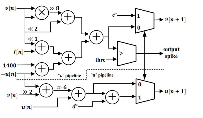
This model captures the essential dynamics of neuronal spiking but can be approximated and transformed into a discrete time equation for FPGA implementation as show in [2], using the following equations:
\[v[n + 1] = \frac{1}{2^8} v^2[n] + 2^2 v[n] + 1400 - u[n] + I[n]\] \[u[n + 1] = u[n] + a^* (b^* v[n] - u[n])\]Where: \(\text{if } v[n + 1] \geq 3000, \text{ then } \begin{cases} v[n + 1] &\leftarrow c^* \\ u[n + 1] &\leftarrow u[n + 1] + d^* \end{cases}\)
In this case, the parameters have been scaled to the following values:
- ( a^* ) = 1/(2^6)
- ( b^* ) = 1/(2^2)
- ( c^* ) = -650
- ( d^* ) = 80
These equations are implemented into the architecture shown below: 
Synaptic Current
The synaptic current is calculated as follows: \(I = \sum_{i} w_i \cdot s_i\)
Where:
- ( I ): Total synaptic current for the given neuron
- ( i ): Index of the input neuron
- ( w_i ): Synaptic weight for the ( i^{th} ) input
- ( s_i ): Spike from the ( i^{th} ) input
When sending an image to the input, pixels are classified as being either black or white. A black pixel will send a constant current to the neuron, while a white pixel will send no current. For the output layer, the spikes generated by the input layer are multiplied by the synaptic weights and summed to produce the total input current for each output neuron, based on the equation above. Thus, there must be a current adding module that can produce the L2 current. For this project, I created two designs: A Low-Latency Current Adder and a Low-Area Current Adder. The Low-Latency Current Adder use an Adder Tree structure to compute partial sums over 10 clock cycles (1 cycle per layer). The Low-Area Current Adder uses 5 adders and a collection of multiplexers to take 8 weights+connections at a time, summing them over 72 clock cycles.
Spiking Neural Network Architecture
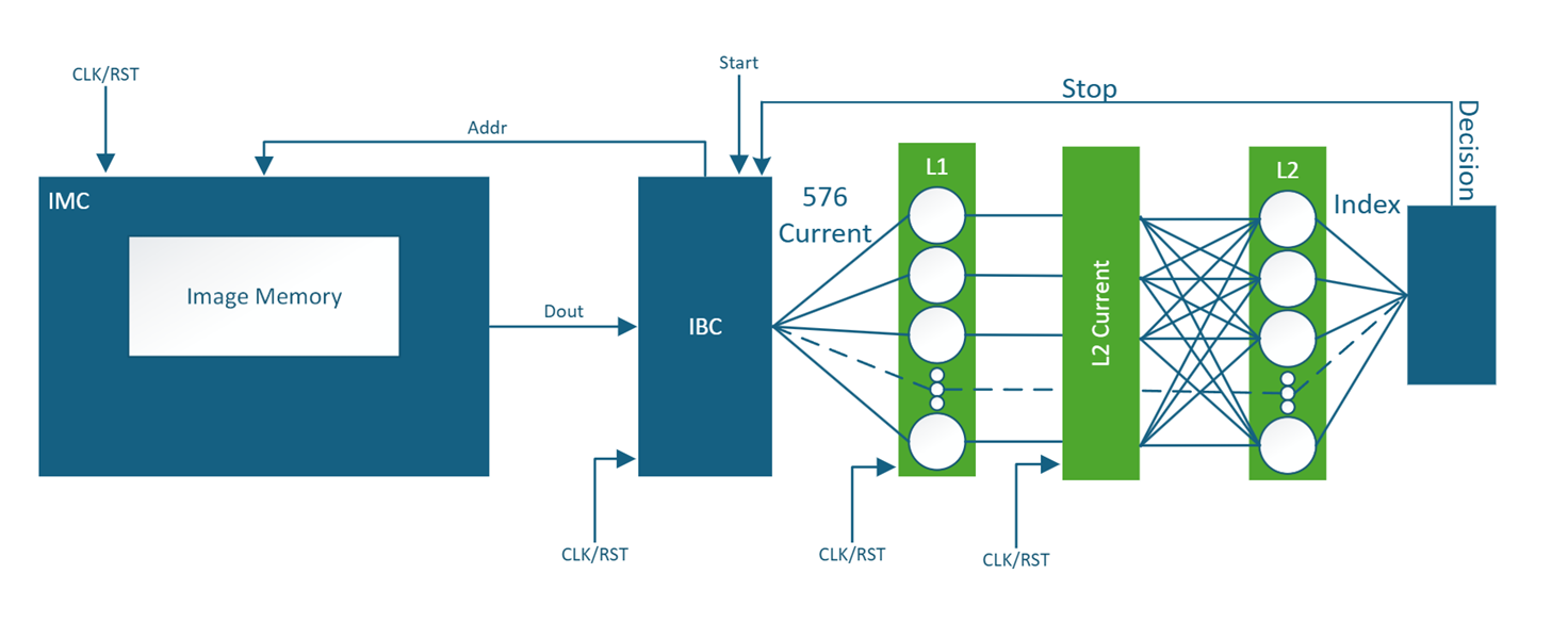
The overall architecture of the SNN is shown below. The input layer consists of 576 Izhekich neurons, each receiving input from a pixel in the 24x24 image. The output layer consists of 48 Izhekich neurons, each fully connected to all input neurons through synaptic weights. The synaptic weights between the input and output layer come from a software trained implementation of the same network, and are stored on ROM in the FPGA. The weights are represented in a fixed-point format to optimize resource usage on the FPGA.  The architecture depicts an Image memory (ROM) and an Input Buffer Controller to facilitate sending images to the network. The input layer then sends spikes to the L2 Current Block, made of 1 of the 2 current adder designs, which computes the synaptic current for each output neuron. The output layer then processes the input current and generates spikes, which are sent to the Output Buffer to store the results. The decision block then analyzes the spikes from the output layer to determine the recognized character.
FPGA Implementation and Results
Using Xilinx Vivado, the SNN targeted the Alveo U50 Data Center Accelerator Card, which features a Xilinx UltraScale+ FPGA. The resource utilization for the project for both current adder designs is as follows:
| Resource Type | Low-Latency Adder | Low-Area Adder | Available |
|---|---|---|---|
| LUTs | 232,025 | 77,464 | 872k |
| Flip-Flops | 303,446 | 45,668 | 1.7M |
| DSPs | 623 | 624 | 5,952 |
Power and Frequency for both designs are as follows:
| Design | Power (W) | Frequency (MHz) |
|---|---|---|
| Low-Latency Adder | 6.087 | 200 |
| Low-Area Adder | 5.198 | 235 |
Compared to [1], the inference latency can be found in the following table:
| Design | Inference Latency |
|---|---|
| Custom RTL [1] | 32 microseconds |
| Low-Latency Adder | 10 microseconds |
| Low-Area Adder | 36 microseconds |
References
- M. A. Bhuiyan, R. Jalasutram and T. M. Taha, “Character recognition with two spiking neural network models on multicore architectures,” 2009 IEEE Symposium on Computational Intelligence for Multimedia Signal and Vision Processing, Nashville, TN, USA, 2009, pp. 29-34, doi: 10.1109/CIMSVP.2009.4925644.
- S. Yang, P. Liu, J. Xue, R. Sun and R. Ying, “An Efficient FPGA Implementation of Izhikevich Neuron Model,” 2020 International SoC Design Conference (ISOCC), Yeosu, Korea (South), 2020, pp. 141-142, doi: 10.1109/ISOCC50952.2020.9333014.
