Optimizing an STDP Learning Engine for FPGAs
Published:
Written by Aaryan Dhawan, in collaboration with Muhammad Farhan Azmine
What is STDP?
Spike-Timing-Dependent Plasticity (STDP) is a biological learning rule that adjusts the strength of connections between neurons based on the relative timing of their spikes. In simple terms within a pair of neurons, if the presynaptic neuron fires before the post synaptic neuron, the connection between them is strengthened. Conversely if the presynaptic neuron fires later than the post synaptic neuron, the connection is weakened. In machine learning, STDP is used to train some Spiking Neural Networks (SNNs) by mimicking this biological process, allowing the network to learn from temporal patterns in data. Using temporal patterns to learn, STDP allows SNNs to process information similarly to the human brain, making them suitable for tasks like real-time learning, robotics, and in edge computing.
On-Chip STDP Learning
On-chip STDP learning refers to the implementation of the STDP learning algorithm directly within machine learning hardware accelerators, rather than training the network in software and transferring it to hardware. This approach is particularly beneficial for applications with limited data availability or when power consumption is a concern. In 2019, researches at Texas A&M University developed FPGA efficient, STDP based SNN models for both supervised and unsupervised learning 1 with Liquid State machines (LSMs). In this work, they build a STDP learning engine that takes the spike timing difference between the current neuron output and the presynaptic neuron, and uses that to determine between strengthening (Potentiation) or weakening (Depression) the connection between the two neurons. This adjustment value is determined by the following equations:
STDP Potentiation and Depression Equations
\(\Delta w = \begin{cases} \eta_{+} \cdot e^{-\frac{t_{pre}-t_{post}}{\tau_{+}}} & \text{if } t_{pre} < t_{post} \\ -\eta_{-} \cdot e^{-\frac{t_{post}-t_{pre}}{\tau_{-}}} & \text{if } t_{pre} > t_{post} \end{cases}\)
where:
- \(\Delta w\) is the change in weight
- \(t_{pre}\) is the time of the pre-synaptic spike
- \(t_{post}\) is the time of the post-synaptic/current neuron spike
- \(\tau_{+}\) is the time constant for potentiation
- \(\tau_{-}\) is the time constant for depression
- \(\eta_{+}\) is the amplitude of the potentiation curve
- \(\eta_{-}\) is the amplitude of the depression curve
Over a given sample period, each neuron will produce a spike train, which is compared against the spike generated from the presynaptic neurons to compute a timing difference values, \(\Delta t\). This \(\Delta t\) is used to calculate the potentiation or depression value, strengthening or weakening a given connection. Determining potentiation vs depression can be visualized as follows:  If the presynaptic neuron spikes before the post-synaptic neuron, the timing difference \(\Delta t\) is positive, indicating that the connection should be strengthened (potentiation). Conversely, if the presynaptic neuron spikes after the post-synaptic neuron, the timing difference \(\Delta t\) is negative, indicating that the connection should be weakened (depression).
Original Hardware Design
In 1, the authors develop a “hardware-friendly STDP learning engine”, recreated in the simplified diagram below. 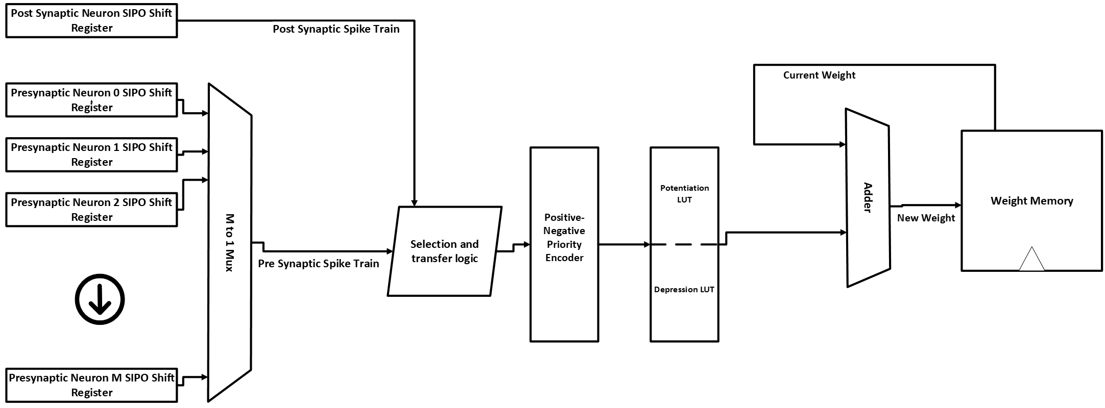 Although the referred diagram from 1 shows a simplified architecture, the actual datapath should be as the following, including the registers within the datapath to avoid metastability issues:
 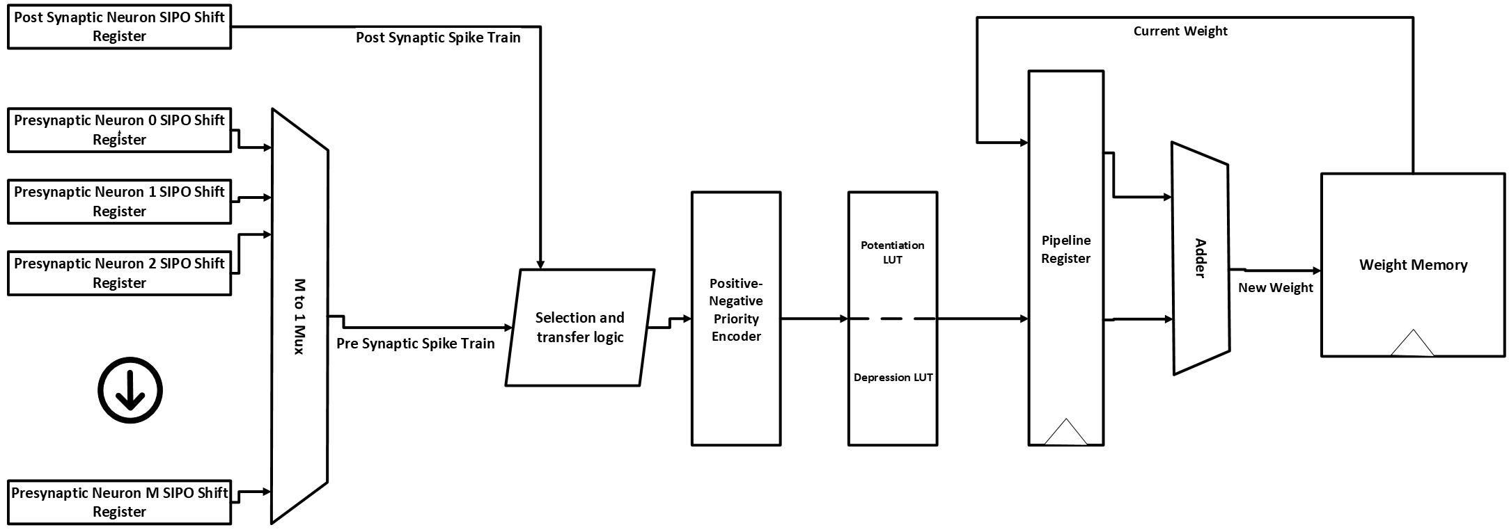 Discrete spike trains from the presynaptic neurons and post-synaptic/current neuron outputs are fed into Serial-In/Parallel-Out (SIPO) shift registers, the “length” of the registers are equal to the length of the timing window memory between the post synaptic spike and the presynaptic spikes. The shift registers corresponding to the presynaptic neurons are then selected by an M to 1 multiplexer, where M is the number of presynaptic neurons connected to the current post synaptic neuron, which possessing the learning engine. Once one of the presynaptic shift registers is selected and its data is passed through the multiplexer, the contents of the selected presynaptic and the post synaptic shift registers are compared to each other to determine the \(\Delta t\) to adjust that given weight. This is done by comparator, which looks at the Most Significant bit(MSB) of the two spike trains and looks at which of the two is high/Logic-1. If the Pre-synaptic shift register MSB is high, the content of the post-synaptic shift register will be sent to the priority encoder and the produced output \(\Delta t\) will be a negative timing difference. Vice versa, if the Post-synaptic shift register MSB is high, the content of the pre-synaptic shift register will be sent to the priority encoder and the produced output \(\Delta t\) will be a positive timing difference. We can model this design in the following verilog code:
always_ff @(posedge clk) begin
        if (rst) begin
            data_reg <= 16'b0;
            flag <= 1'b0;
            LUT_out_reg <= 20'b0;
        end else begin
            if(Post[15]==1) begin
                data_reg <= Pre;
                flag <= 1'b0; // Post-synaptic neuron is active, set flag to 0
            end
            else if (Pre[15] == 1) begin
                data_reg <= Post;
                flag <= 1'b1; // Pre-synaptic neuron is active, set flag to 1
            end
            else begin
                data_reg <= 16'b0; // No active neuron, reset to zero
                flag <= 1'b0; // Reset flag
            end
            // Update LUT output register
            LUT_out_reg <= LUT_out; // Store LUT output in register
        end
    end

    always_comb begin
        if(flag) begin
            unique casez(data_reg)
                16'b1???????????????: TimingDifference = 6'sd0; // 0
                16'b01??????????????: TimingDifference = 6'sd1; // 1
                16'b001?????????????: TimingDifference = 6'sd2; // 2
                16'b0001????????????: TimingDifference = 6'sd3; // 3
                16'b00001???????????: TimingDifference = 6'sd4; // 4
                16'b000001??????????: TimingDifference = 6'sd5; // 5
                16'b0000001?????????: TimingDifference = 6'sd6; // 6
                16'b00000001????????: TimingDifference = 6'sd7; // 7
                16'b000000001???????: TimingDifference = 6'sd8; // 8
                16'b0000000001??????: TimingDifference = 6'sd9; // 9
                16'b00000000001?????: TimingDifference = 6'sd10; // 10
                16'b000000000001????: TimingDifference = 6'sd11; // 11
                16'b0000000000001???: TimingDifference = 6'sd12; // 12
                16'b00000000000001??: TimingDifference = 6'sd13; // 13
                16'b000000000000001?: TimingDifference = 6'sd14; // 14
                16'b0000000000000001: TimingDifference = 6'sd15; // 15
                default:              TimingDifference = 6'sd0; // Default case
            endcase
        end
        else if (!flag) begin
            unique casez(data_reg)
                    16'b1???????????????: TimingDifference = -6'sd0; // 0
                    16'b01??????????????: TimingDifference = -6'sd1; // 1
                    16'b001?????????????: TimingDifference = -6'sd2; // 2
                    16'b0001????????????: TimingDifference = -6'sd3; // 3
                    16'b00001???????????: TimingDifference = -6'sd4; // 4
                    16'b000001??????????: TimingDifference = -6'sd5; // 5
                    16'b0000001?????????: TimingDifference = -6'sd6; // 6
                    16'b00000001????????: TimingDifference = -6'sd7; // 7
                    16'b000000001???????: TimingDifference = -6'sd8; // 8
                    16'b0000000001??????: TimingDifference = -6'sd9; // 9
                    16'b00000000001?????: TimingDifference = -6'sd10; // 10
                    16'b000000000001????: TimingDifference = -6'sd11; // 11
                    16'b0000000000001???: TimingDifference = -6'sd12; // 12
                    16'b00000000000001??: TimingDifference = -6'sd13; // 13
                    16'b000000000000001?: TimingDifference = -6'sd14; // 14
                    16'b0000000000000001: TimingDifference = -6'sd15; // 15
                    default:              TimingDifference = -6'sd0; // Default case
                endcase
        end
Rather than implementing hardware to compute the potention/depression values with the 2 equations above, the authors use a single Look-Up Table (LUT), containing both positive and negative values to easily compute \(\Delta w\) as there is only a certain range of possible values. \(\Delta w\) is then added to synaptic connection, read from a memory block, using a simple adder. The synaptic connection is then written back to the memory block, completing the learning process for that given connection. The LUT and Adder are implemented as follows:
 unique casez(TimingDifference)
            -'sd15:  LUT_out = -'sd22;
            -'sd14:  LUT_out = -'sd25;
            -'sd13:  LUT_out = -'sd27;
            -'sd12:  LUT_out = -'sd30;
            -'sd11:  LUT_out = -'sd33;
            -'sd10:  LUT_out = -'sd37;
            -'sd9:   LUT_out = -'sd41;
            -'sd8:   LUT_out = -'sd45;
            -'sd7:   LUT_out = -'sd50;
            -'sd6:   LUT_out = -'sd55;
            -'sd5:   LUT_out = -'sd61;
            -'sd4:   LUT_out = -'sd67;
            -'sd3:   LUT_out = -'sd74;
            -'sd2:   LUT_out = -'sd82;
            -'sd1:   LUT_out = -'sd90;
             'sd0:   LUT_out =  'sd0;
             'sd1:   LUT_out =  'sd90;
             'sd2:   LUT_out =  'sd82;
             'sd3:   LUT_out =  'sd74;
             'sd4:   LUT_out =  'sd67;
             'sd5:   LUT_out =  'sd61;
             'sd6:   LUT_out =  'sd55;
             'sd7:   LUT_out =  'sd50;
             'sd8:   LUT_out =  'sd45;
             'sd9:   LUT_out =  'sd41;
             'sd10:  LUT_out =  'sd37;
             'sd11:  LUT_out =  'sd33;
             'sd12:  LUT_out =  'sd30;
             'sd13:  LUT_out =  'sd27;
             'sd14:  LUT_out =  'sd25;
             'sd15:  LUT_out =  'sd22;
            default: LUT_out =  'sd0;
        endcase
        NewW = CurrentW + LUT_out_reg;
Optimizing the Learning Engine
Looking at this design, we can identify a few areas for optimization, specifically in the timing difference calculation and the potentiation/depression value calculation. Seeing that the depression values are simply the negative of the potentiation values, we can reduce the LUT size by only storing the absolute weight change values and using a signed flag to determine if the value should be added or subtracted from the current weight. Moreover, we can then simplify the priority encoder size since it only needs to generate the absolute value of the timing difference, rather than both positive and negative values, and add simple logic to generate the signed flag.
Optimizations:
- Reduce the Potentiation/Depression LUT size
- Replace a priority encoder with a single-bit, flag signal.
This results in the following design 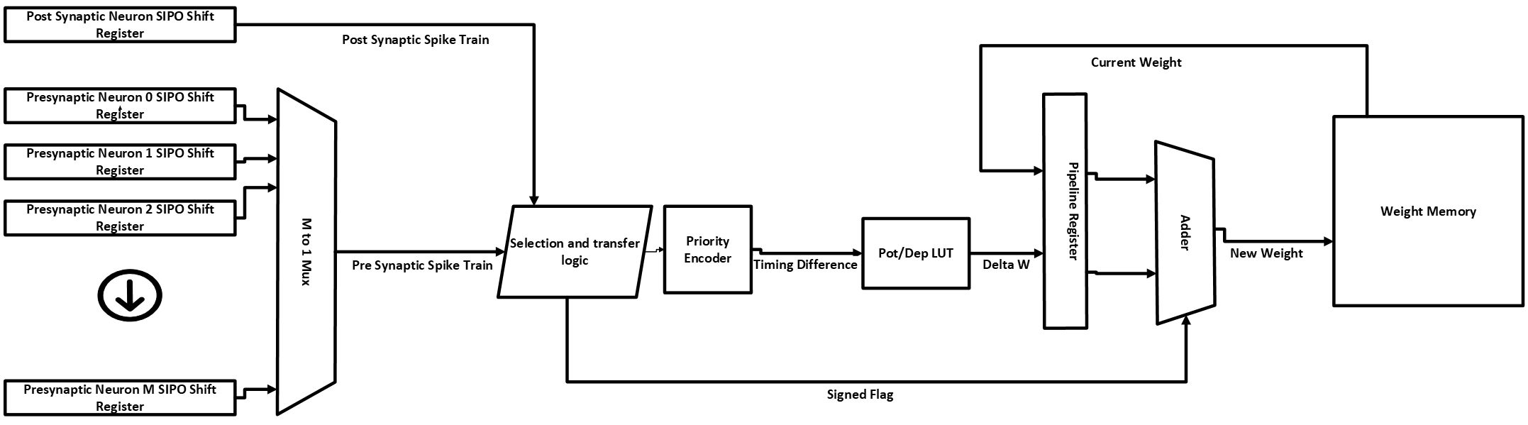
Below is the simplified Verilog code for the optimized priority encoder and signed flag logic:
logic [15:0] data_reg;
    always_ff @(posedge clk) begin
        if (rst) begin
            data_reg <= 16'b0;
            SignedFlag <= 0; // Reset SignedFlag on reset
        end else begin
            if (PostSynapticNeuron[15] == 1) begin
                data_reg <= PreSynapticNeuron;
                SignedFlag <= 0; // PostSynapticNeuron is active, set SignedFlag
            end else if (PreSynapticNeuron[15] == 1) begin
                data_reg <= PostSynapticNeuron;
                SignedFlag <= 1; // PreSynapticNeuron is active, set SignedFlag
            end
        end
    end

    always_comb begin
        unique casez(data_reg)
            16'b1???????????????: TimingDifference = 4'd0; // 0
            16'b01??????????????: TimingDifference = 4'd1; // 1
            16'b001?????????????: TimingDifference = 4'd2; // 2
            16'b0001????????????: TimingDifference = 4'd3; // 3
            16'b00001???????????: TimingDifference = 4'd4; // 4
            16'b000001??????????: TimingDifference = 4'd5; // 5
            16'b0000001?????????: TimingDifference = 4'd6; // 6
            16'b00000001????????: TimingDifference = 4'd7; // 7
            16'b000000001???????: TimingDifference = 4'd8; // 8
            16'b0000000001??????: TimingDifference = 4'd9; // 9
            16'b00000000001?????: TimingDifference = 4'd10; // 10
            16'b000000000001????: TimingDifference = 4'd11; // 11
            16'b0000000000001???: TimingDifference = 4'd12; // 12
            16'b00000000000001??: TimingDifference = 4'd13; // 13
            16'b000000000000001?: TimingDifference = 4'd14; // 14
            16'b0000000000000001: TimingDifference = 4'd15; // 15
            default:              TimingDifference = 4'd0; // Default case
        endcase
    end
The potentiation LUT is now reduced to 16 entries, as the depression values are not needed. The adder now takes in the absolute weight change value and a signed flag, which determines if the value should be added/subtracted from the current weight according to potentiation/depression. The adder and LUT can be implemented as follows:
always_comb begin
      unique case (potDepIndex)
        4'd0: potDepValue = 'sd0;
        4'd1: potDepValue = 'sd90;
        4'd2: potDepValue = 'sd82;
        4'd3: potDepValue = 'sd74;
        4'd4: potDepValue = 'sd67;
        4'd5: potDepValue = 'sd61;
        4'd6: potDepValue = 'sd55;
        4'd7: potDepValue = 'sd50;
        4'd8: potDepValue = 'sd45;
        4'd9: potDepValue = 'sd41;
        4'd10: potDepValue = 'sd37;
        4'd11: potDepValue = 'sd33;
        4'd12: potDepValue = 'sd30;
        4'd13: potDepValue = 'sd27;
        4'd14: potDepValue = 'sd25;
        4'd15: potDepValue = 'sd22;
        default: potDepValue = 'sd0;
    endcase
end
   always_comb begin
        NewW = CurrentW + (SignedFlag ? -DeltaW : DeltaW); // SignedFlag = 1 means subtract
    end
FPGA Utilization
We designed, synthesized, and implemented the original and optimized STDP learning engines on a Xilinx Zynq-7000 SoC “ZC702” Evaulation board. The following table shows the FPGA resource utilization for both designs:
| Resource Type | Original Design | Optimized Design |
|---|---|---|
| LUTs | 179 | 141 |
| FFs | 347 | 341 |
| Fmax | 187 MHz | 205 MHz |
From the table, we can see that the optimized design has reduced LUT utilization by 23.75% and increase the Fmax by 10.25% due to reduction in the critical path, while manintaing the a similar number of flip-flops (FFs).
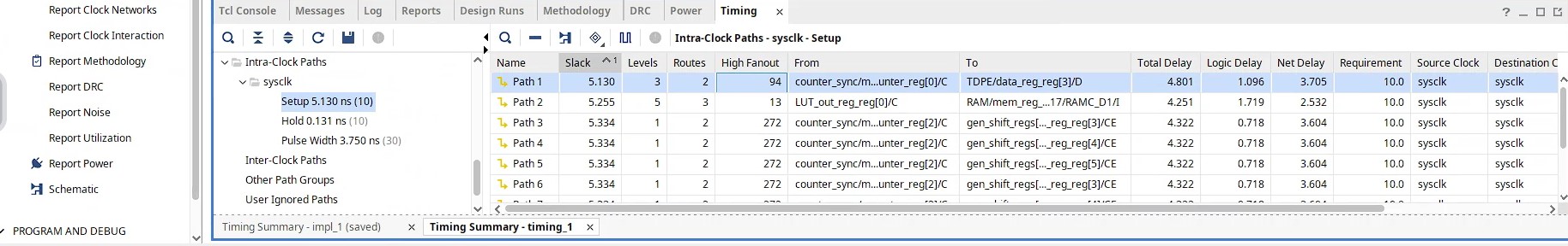
Critical Path Analysis
To understand the increase in Fmax, we can analyze the critical path of both designs. The critical path is the longest path delay through the circuit that determines the maximum frequency at which the circuit can operate. In the original design, the critical path reported from Vivado is 5.393 ns as shown in the attached image from Vivado’s Timing Summary. 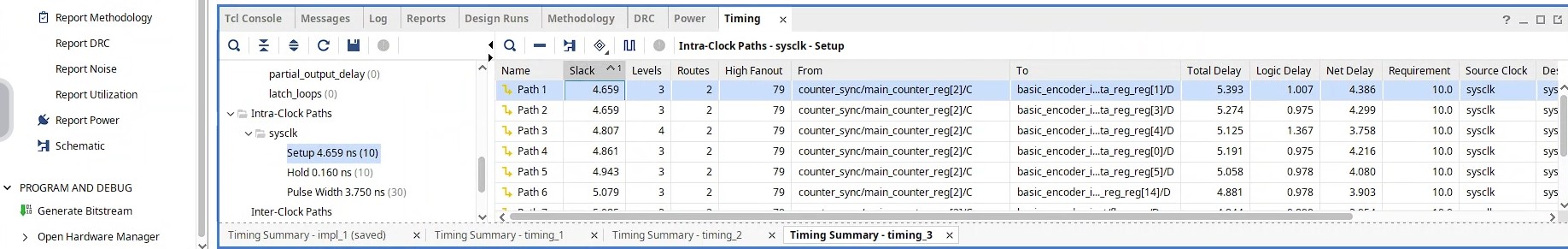 In the optimized design, the critical path is reduced to 4.801 ns, shown in the Vivado Timing Summary below.